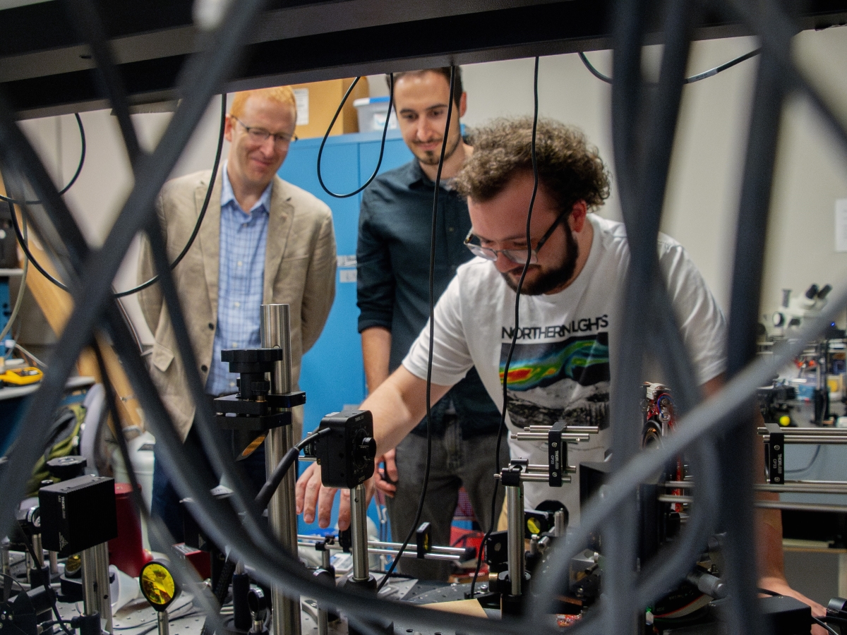
Professor Dan Wasserman with Zarko Sakotic and Noah Mansfield in the lab.
Texas Engineers have demonstrated a technique to trick light into behaving as if it was interacting with atomically thin metal films, setting the stage for the design and development of next-generation optoelectronic devices such as emitters, detectors and nano-sensors that could be used in health care, pollution detection, telecommunications and more.
Using only off-the-shelf materials and lithographic patterning, the researchers developed a novel technique they call “infrared metaplasmonics.” This technique, published recently in ACS Photonics, enables structures that can confine long-wavelength light down to nano-scale dimensions, unlocking new opportunities to leverage the largely untapped infrared light spectrum.
The metaplasmonic structures demonstrated by the team can confine light to dimensions as small as 1/100th of the wavelength of light. They offer a tantalizing opportunity to engineer light-matter interaction in ultra-small volumes, essential for bridging the gap between the length scales of light and electronic and quantum structures.
Plasmonics involves using metals to trap and guide light at scales much smaller than the wavelength of the light itself. This ability to confine light at the nanoscale is crucial for technologies like sensors and optical circuits. However, traditional plasmonic materials, such as gold and silver, can only achieve this confinement at visible wavelengths, leaving infrared light largely untapped.
The work was inspired by recent demonstrations of atomically thin metals for optical applications. This work showed that such metals could support optical modes known as surface plasmons at much longer wavelengths than traditional, thick metal films. However, growing high-quality metal films so thin is extremely challenging, and even when they are grown at their highest, single-crystal quality, losses intrinsic to the atomic-scale thickness dominate the optical response.
“Metal films acquire many appealing optical properties once they are thinned down to the atomic scale, and a lot of it has to do with the massively decreased number of electrons interacting with light,” said Zarko Sakotic, a research associate who led the research with professor Dan Wasserman in the Chandra Family Department of Electrical and Computer Engineering. “However, it also means that the electrons in the film bounce off the surface of the metal, causing significant losses known as Landau damping. So, we thought, instead of thinning it, maybe we can remove a large fraction of the metal film, essentially diluting it, and trick light into thinking it was interacting with an atomically thin film.”

Daniel Wasserman, professor in the Cockrell School of Engineering’s Chandra Family Department of Electrical and Computer Engineering
The team grew thicker, 30-nanometer metal films but patterned them with ultra-small but dense perforations. They removed so much metal that the remaining metal volume approximated that of an atomically thin film. They then shaped these films into 100-nanometer nano-ribbons that act like antennas for light with wavelengths up to 10 micrometers, or 100x the size of the nano-ribbon.
“Zarko’s insight was really clever. Building on some of his earlier published work in the group, Zarko realized that as long as he perforated a metal film on length scales much smaller than the wavelength of light, incident light would not be able to tell whether it was interacting with a thick metal film with large chunks missing, or a metal film only a few atomic layers thick,” said Wasserman. “But he also quickly realized that the thicker metaplasmonic films would have much lower loss, because the electrons in the films were not constrained by the atomic-scale thickness of the metal. So metaplasmonics does more than mimic a difficult-to-synthesize material, it significantly improves on the optical properties of those materials.”
The metaplasmonic film confined infrared light an order of magnitude more tightly than traditional materials. Numerical simulations suggest that this confinement could be increased even further, up to two orders of magnitude. Importantly, the films maintain high optical quality, avoiding the energy losses that typically plague ultra-thin materials.
Infrared light plays a vital role in many aspects of modern life. It is used in thermal cameras to detect heat, in fiber-optic networks to transmit data, and in medical devices to monitor health. The ability to manipulate infrared light more efficiently could lead to significant advancements in these areas.
For example, metaplasmonic materials could improve the sensitivity of infrared sensors, enabling more accurate detection of gases or pollutants. In health care, they could enhance imaging technologies, making it easier to diagnose diseases or monitor vital signs. In telecommunications, they could pave the way for faster and more reliable data transmission.
“What we have demonstrated,” Sakotic said, “is an effective material system whose optical properties we can tune by design, so we are looking to engineer these metaplasmonic materials to match a wide range of applications such as next-generation sensors and sources. At the same time, the ability to control metal properties by design at these wavelengths offers us the opportunity to explore unique optical phenomena with a degree of control that is simply not possible with off-the-shelf materials.”
The team also included graduate students Noah Mansfield, Amogh Raju, Alexander Ware, Divya Hungund, and Daniel Krueger from Wasserman’s Mid-IR Photonics Lab.